Solar power is transforming the way we generate electricity, and at the core of this revolution are photovoltaic (PV) cells—the devices that convert sunlight into usable energy. But not all solar cells are built the same. Their structure, efficiency, and cost depend largely on the crystallinity of their semiconductor materials. In this article, we’ll break down the major types of PV cells, focusing on how their crystal structures are formed and how that impacts their performance.
Monocrystalline Silicon (Mono-Si) Solar Cells
Structure: Single-Crystal Silicon
Monocrystalline solar cells are made from a single continuous crystal of silicon, meaning the silicon atoms are arranged in a perfect, uniform lattice. This ordered structure allows for high electron mobility, reducing energy loss and making these cells the most efficient on the market
Formation Process: The Czochralski Method
To create monocrystalline silicon:
- A small seed crystal of silicon is dipped into molten silicon.
- The seed is slowly pulled up while rotating, allowing a single crystal (or ingot) to form.
- This large cylindrical ingot is then sliced into thin wafers to create solar cells.
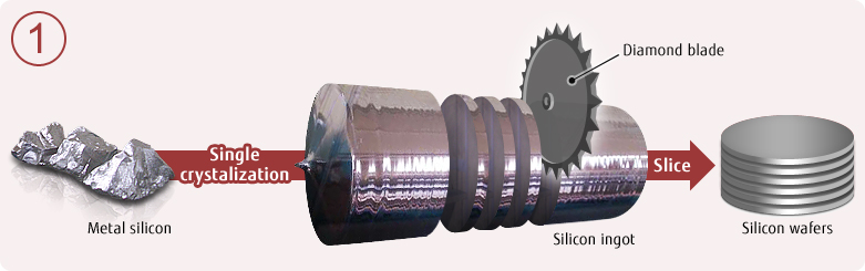
The wafer surfaces are then chemically etched and textured to create tiny pyramidal structures that reduce light reflection. Without this, silicon would reflect about 35% of incoming sunlight, which is bad for solar efficiency.
A thin layer of silicon nitride (Si₃N₄) or titanium dioxide (TiO₂) is applied to the wafer. This anti-reflective coating (ARC) further reduces reflection to just 1-2% and gives monocrystalline solar cells their signature dark blue to black color. The exact color depends on the thickness and composition of the coating.
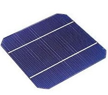
Key Features:
- Efficiency: 18-22% (higher in lab conditions)
- Appearance: Uniform black color, due to the smooth crystal structure
- Durability: 25+ years of lifespan
- Cost: High, due to the energy-intensive manufacturing process
Best for: Homeowners and businesses looking for maximum efficiency and longevity in their solar investment.
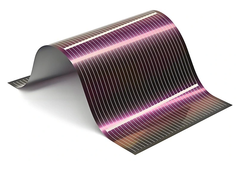
Polycrystalline Silicon (Poly-Si) Solar Cells
Structure: Multi-Crystal Silicon
Unlike monocrystalline cells, polycrystalline cells are made of many small silicon crystals fused together. This results in a grainy structure with crystal boundaries that slightly impede electron movement, lowering efficiency.
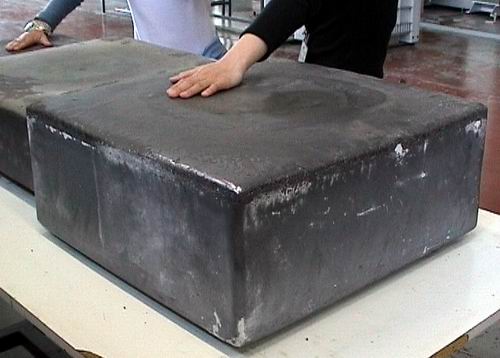
Formation Process: Cast Silicon Method
- Molten silicon is poured into a mold rather than being pulled into a single crystal.
- As it cools, multiple silicon crystals form randomly, creating a grainy, non-uniform structure.
- The solidified silicon block is then cut into wafers for solar cell production.
The wafer surfaces are then chemically etched and textured to create a randomized texture that helps reduce light reflection. Unlike monocrystalline wafers, which have a uniform pyramid pattern, polycrystalline wafers have an irregular texture due to their multi-crystal structure.
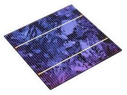
Key Features:
- Efficiency: 15-18% (lower than monocrystalline due to grain boundaries)
- Appearance: Bluish hue with visible crystal grains
- Durability: Similar to monocrystalline but slightly lower performance in extreme heat
- Cost: Lower than monocrystalline, as the manufacturing process is simpler and wastes less material
Best for: Those looking for a budget-friendly solar option with decent efficiency.
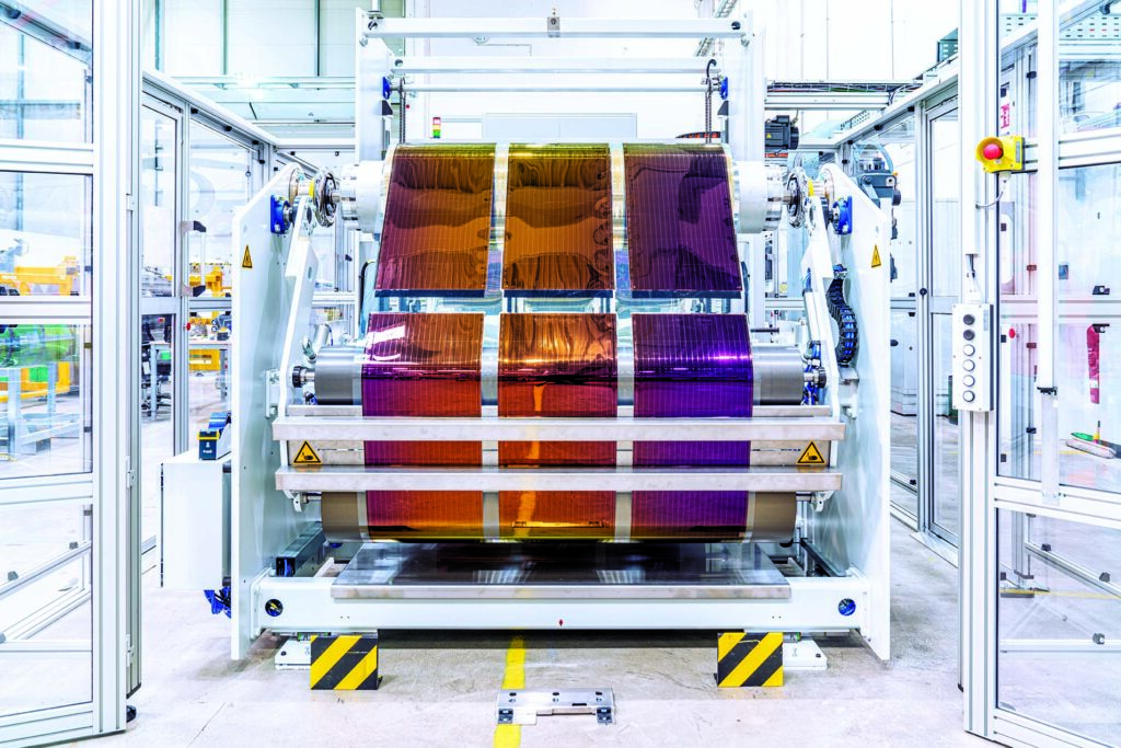
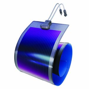
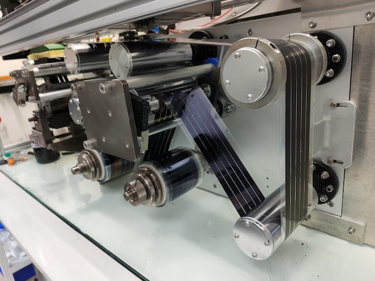
Thin-Film Solar Cells: The Flexible Alternative
Structure: Non-Crystalline or Polycrystalline Thin Layers
Thin-film solar cells differ from crystalline silicon (c-Si) solar panels because they don’t use bulk silicon wafers. Instead, they are made by depositing extremely thin layers (a few micrometers thick) of photovoltaic material onto a substrate like glass, plastic, or metal.
Formation Process: Vapor Deposition & Sputtering
- Thin layers of photovoltaic materials are deposited using chemical vapor deposition (CVD) or sputtering techniques.
- The process is fast and uses much less material, making thin-film panels cheaper and more adaptable to different surfaces.
There are several types of thin-film solar cells, depending on the material used:
A. Amorphous Silicon (a-Si) Solar Cells
- Structure: Non-crystalline silicon, where atoms are randomly arranged instead of forming a lattice.
- Pros: Cheap, flexible, works better in low light.
- Cons: Low efficiency (~6-12%), degrades faster.
- Best for: Consumer electronics, flexible panels, low-power applications.
B. Cadmium Telluride (CdTe) Solar Cells
- Structure: Polycrystalline CdTe semiconductor.
- Pros: Higher efficiency (16-18%), lower production costs than silicon.
- Cons: Toxic cadmium content, environmental concerns.
- Best for: Large-scale utility projects.
C. Copper Indium Gallium Selenide (CIGS) Solar Cells
- Structure: Polycrystalline semiconductor combining Cu, In, Ga, and Se.
- Pros: Highest efficiency among thin-films (17-20%), flexible.
- Cons: Expensive to produce.
- Best for: High-performance flexible applications, space-constrained rooftops.
Perovskite Solar Cells: The Next Generation
Structure: Hybrid Organic-Inorganic Perovskite Crystals
Perovskite solar cells use a unique crystal structure (ABX₃), where:
- A is an organic or inorganic cation (e.g., methylammonium).
- B is a metal cation (e.g., lead or tin).
- X is a halide anion (e.g., iodine or bromine).
Unlike silicon, perovskite crystals self-assemble at low temperatures, making them cheaper to produce.
Formation Process: Solution Processing
- Perovskite precursors are dissolved in a liquid solution and then deposited onto a substrate.
- The material crystallizes on its own, forming a thin, efficient photovoltaic layer.
Key Features:
- Efficiency: Over 25% (rapidly improving)
- Cost: Very low potential production costs
- Flexibility: Can be printed or sprayed onto surfaces
- Durability Issues: Susceptible to moisture, stability still being researched